


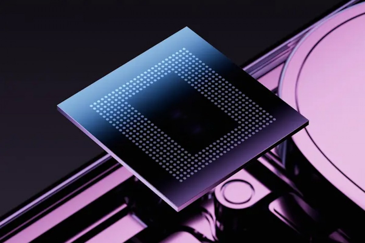
A brand new report from Android Authority particulars the upcoming Pixel 10 collection’ customized Tensor G5 chipset. The brand new report corroborates earlier claims that the G5 shall be designed by Google and fabbed by TSMC as a substitute of Samsung and we get much more particulars on the parts contained in the upcoming chip.
Tensor G5 shall be fabbed on TSMC’s 3nm-class node and Google will use Arm Cortex CPU cores. The massive distinction on the G5 is that Google will go for an Creativeness Applied sciences GPU, particularly the IMG DXT, which replaces the Arm Mali-G715 MP7 from the Tensor G4.
The opposite notable change is the absolutely customized picture sign processor (ISP), which is able to change the partially customized designs of its predecessors, which relied on modified Samsung ISPs with Google-designed blocks. Ever since switching to Tensor chips, Google has not used a completely customized ISP in its Pixel telephones so this variation needs to be an enormous one for digital camera efficiency.
Google can be anticipated to make use of a customized reminiscence controller, system-level cache and energy modules.
Elsewhere, Google will go away from its customized “BigWave” AV1 video codec and Samsung’s MFC (Multi Format Codec) and can as a substitute depend on Chips&Media’s WAVE677DV which helps encoding and decoding in AV1, VP9, HEVC and H.264 codecs.
Tensor G5 can be anticipated to characteristic third-party USB, PCIe, and I3C parts in addition to third-party interfaces for the DSI (show), DisplayPort, flash storage and reminiscence (LPDDR5x).


